Printed circuit boards are just one of many products we at Hallmark Nameplate produce, with the highest quality and efficiency in mind. We’re here to educate you on the functionality and purpose of a circuit board so you fully understand our processes as well as your needs.
A printed circuit board mechanically supports and electrically connects electronic components using conductive tracts, pads and other features etched from copper sheets laminated onto a non-conductive substrate. PCBs can be single sided, double sided, or multi-layered. Multi-layered PCBs allow for much higher component density. Conductors on different layers are connected with plated-through holes called “vias”. Advanced PCBs may contain components, such as capacitors, resistors, or active devices, embedded in the substrate.
Printed circuit boards are used in all but the simplest electronic products. Alternatives to PCBs include wire wrap and point to point construction. PCBs require the additional design effort to lay out the circuit, but manufacturing and assembly can be automated. Manufacturing circuits with PCBs is cheaper and faster than with other wiring methods as components are mounted and wired with one single part. Furthermore, operator wiring errors are eliminated.
When the board has only copper connections and no embedded components, it is more correctly called a wiring board or etched wiring board. Although more accurate, the term printed wiring board has fallen into disuse. A PCB populated with electronic components is called a printed circuit assembly, printed circuit board assembly or PCB assembly. The IPC preferred term for assembled boards is circuit card assembly, and for assembled backplanes, it is backplane assemblies. The term PCB is used informally both for bare and assembled boards.
The world market for bare PCBs reached nearly $60 billion in 2012.
Much of the electronics industry’s PCB design, assembly, and quality control follows standards published by the IPC organization.
Through-Hole Technology
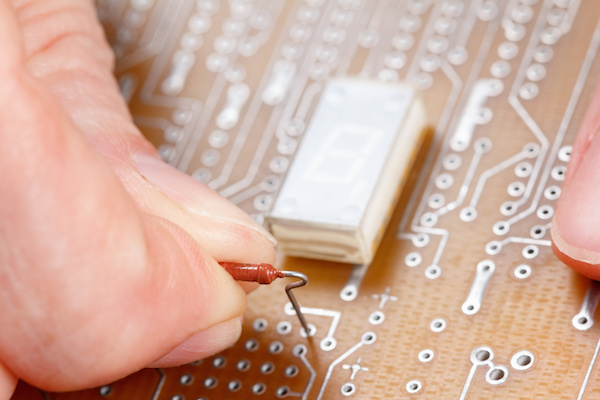
The first PCBs used through-hole technology, mounting electronic components by leads inserted through holes on one side of the board and soldered onto copper traces on the other side. Boards may be single-sided, with an unplated component side, or more compact double-sided boards, with components soldered on both sides. Horizontal installation of through-hole parts with two axial leads (such as resistors, capacitors, and diodes) is done by bending the leads 90 degrees in the same direction, inserting the part in the board (often bending leads located on the back of the board in opposite directions to improve the part’s mechanical strength), soldering the leads, and trimming off the ends. Leads may be soldered either manually or by a wave soldering machine.
Through-hole PCB technology almost completely replaced earlier electronics assembly techniques such as point-to-point construction. From the second generation of computers in the 1950s until surface-mount technology became popular in the late 1980s, every component on a typical PCB was a through-hole component.
Surface-Mount Technology
Surface-mount technology emerged in the 1960s, gained momentum in the early 1980s and became widely used by the mid-1990s. Components were mechanically redesigned to have small metal tabs or end caps that could be soldered directly onto the PCB surface, instead of wire leads to pass through holes. Components became much smaller and component placement on both sides of the board became more common than with through-hole mounting, allowing much smaller PCB assemblies with much higher circuit densities.
Circuit Properties of the PCB
Each trace consists of a flat, narrow part of the copper foil that remains after etching. The resistance, determined by width and thickness, of the traces must be sufficiently low for the current the conductor will carry. Power and ground traces may need to be wider than signal traces. In a multi-layer board, one entire layer may be mostly solid copper to act as a ground plane for shielding and power return. For microwave circuits, transmission lines can be laid out in the form of stripline and microstrip with carefully controlled dimensions to assure a consistent impedance. In radio-frequency and fast switching circuits the inductance and capacitance of the printed circuit board conductors become significant circuit elements, usually undesired; but they can be used as a deliberate part of the circuit design, obviating the need for additional discrete components.
Printed circuit boards from Hallmark Nameplate have been rated among the highest quality in North America. We are fully vertically integrated and can take your prototype from design to circuit board to full visual and electronic testing. Hallmark Nameplate’s electronic manufacturing services provide everything you need in the development of your product’s electrical components.


