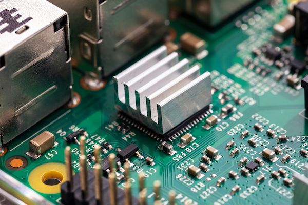
Surface mount technology (SMT) revolutionized the electronics industry by allowing for the creation of smaller, faster, and more reliable devices. Unlike traditional through-hole assembly, the SMT process directly mounts components onto the surface of a printed circuit board (PCB), streamlining production and boosting efficiency.
SMT plays a pivotal role in modern manufacturing, from consumer gadgets to industrial machinery. In this blog, we will dive into the fundamentals of SMT, explore its advantages, outline the SMT process, and explain why it’s a game-changer for original equipment manufacturers (OEMs).
Let’s uncover how SMT shapes today’s electronics!
What is Surface Mount Technology (SMT)?
Surface Mount Technology, also called Planar Mounting, emerged during the 1960s and 1970s as electronics manufacturers sought more efficient ways to assemble components onto circuit boards. Traditional through-hole methods, which required drilling and manual insertion of components, were time-consuming and limited in their ability to support miniaturization.
In 1960, IBM became the first to apply surface mount technology in a small-scale computer system that later guided the Saturn IV and Saturn V vehicles.
SMT revolutionized the industry by enabling components to be placed directly onto the PCB surface. By the 1980s, SMT gained widespread adoption. This fueled the growth of compact consumer electronics like personal computers and mobile devices.
Advantages of SMT
As mentioned above, Surface Mount Technology has revolutionized electronics manufacturing with its efficiency and precision. So, let’s explore the key advantages that make SMT the preferred choice for modern electronic assembly.
- Compact Design: The SMT process places components directly on the PCB, significantly reducing the size and weight of electronic devices.
- Improved Performance: Shorter electrical paths minimize resistance and inductance to improve performance and signal integrity.
- Cost Efficiency: Automation reduces labor costs and speeds up production. SMT also uses smaller components, which often cost less.
- High Component Density: SMT enables more components to fit onto a PCB, allowing for advanced functionality in smaller spaces.
- Reliability: SMT provides better resistance to vibrations and shocks, making it ideal for industries that need durable electronics.
SMT vs SMD
Surface Mount Devices (SMD) are closely related to SMT but are distinct concepts. We know that SMT refers to the manufacturing process of mounting electronic components directly onto the surface of a printed circuit board.
SMD, on the other hand, refers to the actual components designed for SMT. While SMT is the method, SMDs are the parts—such as resistors, capacitors, and microchips—that attach to the board.
When put together, SMT and SMD revolutionize electronics manufacturing by creating smaller, more reliable products.
The 5 Main Steps of the SMT Process
In order to make sure components are accurately and securely placed on the PCB, the SMT process involves several key steps. Generally, the process can be categorized into three stages: solder paste printing, components placement, and reflow soldering.
However, to provide a more detailed explanation of the manufacturing process, we’ve outlined the five main steps.
1. SMC and PCB Preparation
The first step involves preparing both the Surface Mount Components (SMCs) and the printed circuit board. In this phase, the components are selected and the PCB is designed.
The PCB is thoroughly cleaned to remove dust, oils, or other contaminants that could interfere with the soldering process. Any oxidation on the board’s surface is removed to ensure proper adhesion of the solder paste.
Meanwhile, SMCs are sorted, inspected, and prepared for assembly. This stage also involves verifying component placement through design files to maintain compatibility and alignment.
2. Solder Paste Printing
Next, a thin layer of solder paste is applied by a printer to the PCB in specific areas where components will sit. This is accomplished using a stencil that matches the circuit design, ensuring precision in the application.
The paste is a mixture of powdered solder and flux, designed to hold components temporarily in place and establish a reliable electrical connection once heated. The quality and accuracy of this step are critical for strong bonds and minimizing defects later.
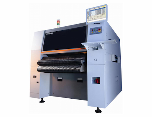
3. Placing the Components
In this stage, a high-speed pick-and-place machine positions the components onto the solder-pasted areas of the PCB. These machines use advanced vision systems to detect, align, and place components with incredible precision. Some machines can operate at speeds up to 200,000 components per hour!
Because even minor misalignments can cause connectivity issues during soldering, this step demands incredible accuracy.
4. Reflow Soldering
After placing the components, the assembled PCB passes through a reflow oven, where it is subjected to carefully controlled heat profiles. This heat melts the solder paste, forming a solid bond between the PCB and the components.
The oven gradually heats the board to avoid thermal stress, then cools it down to solidify the connections. Reflow soldering forms a durable and reliable bond that can withstand the rigors of operation.
5. Cleaning and Inspection
After soldering, the board undergoes cleaning to remove flux residues and other contaminants. Next, the inspection process follows, which may involve automated optical inspection (AOI), X-ray testing, or manual checks. These techniques verify that components are correctly placed, solder joints are secure, and no defects exist, such as bridges or open circuits.
As you can see, the SMT process guarantees that PCBs meet the high standards required for modern electronics. Each step is a vital link in creating reliable and efficient devices.
The Future of SMT
With the demand for smaller, more powerful electronic devices, the future of SMT will evolve to accommodate ultra-miniature components and multi-functional PCBs. Automation, including AI and machine learning, will enhance precision in component placement and defect detection to improve efficiency and reduce errors.
Additionally, the electronics industry is exploring eco-friendly materials and processes to address environmental concerns. These innovations will ensure SMT remains vital in the rapidly evolving electronics landscape.
SMT Solutions Tailored for Your Business
As you can see, Surface Mount Technology has transformed how electronic devices are manufactured, delivering efficiency, precision, and adaptability. From the careful preparation of components and PCBs to the high-tech processes of solder paste application, reflow soldering, and inspection, SMT ensures reliability and performance. With its evolving potential to meet modern demands, SMT remains at the forefront of innovation.
At Hallmark Nameplate, we are proud to support your manufacturing needs with expert solutions and unmatched quality. Let us help you stay ahead—visit our website for a free quote today!