60-years-of-experience

60+ Years of Experience

satisfaction-guarantee

Satisfaction Guarantee

short-lead-times

Short Lead Times

The Basics of Printed Circuit Boards

For all the wonders of electricity, it’s hard to forget that it takes something very physical to make the “magic” happen. That factor is printed circuit boards (PCBs), which have long been the foundation of electrical engineering.

Printed circuit boards are essential components in the world of electronics. They serve as the backbone for countless electronic devices, ranging from smartphones and computers to medical equipment and automotive systems. Regardless of its size, no electrically powered device will work without a PCB of some kind.

Whether it be a cell phone, a remote control, something as complicated as a computer, or as simple as a child’s toy, a PCB provides connectivity between all of the components of a device. As a result, the device will function as it should.

In this article, we embark on a journey to explore the fundamentals of printed circuit boards. We’ll delve into their structure, their function, and unravel the mystery of how these boards enable the operation of our modern electronics.

Let’s begin!

how does a circuit board work

What Are PCBs?

At its core, a PCB is a flat board made of non-conductive material, typically fiberglass-reinforced epoxy laminate, with conductive pathways etched or printed onto its surface. Electrical components are soldered onto the PCB through either wave soldering or selective soldering. Then, a conformal coating is then added to protect the surface and secure its longevity.

The primary purpose of printed circuit boards is to provide a reliable platform for interconnecting electronic components compactly and efficiently. By routing electrical signals between components through predefined pathways, PCBs facilitate the functioning of complex electronic systems with precision and reliability.

The History of PCBs

The origins of printed circuit boards can be traced back to the early 20th century. Before the invention of PCBs, electronic circuits were constructed using cumbersome and unreliable methods such as point-to-point wiring and terminal strips. These methods were labor-intensive and prone to errors and failures, so innovation was necessary.

Early Development

The concept of a printed wiring board, which would later evolve into the modern PCB, emerged in the early 20th century. In 1925, Charles Ducas filed a patent for a method of electrically connecting electronic components using a conductive foil pattern printed on an insulating board. This laid the foundation for the development of PCB technology.

During World War II, the demand for more efficient and reliable electronic systems spurred further advancements in PCB technology. In 1943, Paul Eisler, an Austrian engineer, is credited with creating the first true printed circuit board. Eisler’s invention, known as the “printed wiring,” was used in proximity fuses for anti-aircraft shells used by the Allied forces.

Evolution of Printed Circuit Boards

Following World War II, PCB technology continued to evolve rapidly. The introduction of new materials and manufacturing processes led to significant improvements in PCB design and performance.

1950s

One of the key milestones in the evolution of PCB technology was the development of the “through-hole” method in the 1950s. This method involved drilling holes in the PCB substrate and inserting component leads through the holes before soldering them in place. The through-hole method allowed for more secure connections and improved reliability compared to earlier methods.

1960s-1970s

In the 1960s and 1970s, the introduction of automated assembly techniques such as wave soldering and surface mount technology (SMT) revolutionized PCB manufacturing. Surface mount technology, in particular, allowed for smaller and lighter electronic devices by eliminating the need for bulky through-hole components.

1980s

The 1980s saw the widespread adoption of computer-aided design (CAD) software for PCB design, further enhancing the precision and complexity of PCB layouts. This era also saw the emergence of multi-layer PCBs, which allowed for denser component placement and improved signal integrity.

Recent Years

In recent years, advancements in materials science, manufacturing processes, and miniaturization techniques have continued to drive innovation in PCB technology. High-density interconnect (HDI) PCBs, flexible PCBs, and integrated passive devices (IPDs) are just a few examples of the latest developments pushing the boundaries of what is possible with printed circuit boards.

As you can see, PCBs have played a vital role in shaping the modern world of electronics from its humble beginnings to modern cutting-edge technology. Now, let’s discuss the importance of these electronic boards in our modern world.

The Importance of PCBs in the Electronics Industry

electronics

The importance of PCBs in the electronics industry cannot be overstated. Virtually every electronic device relies on PCBs to function, making them indispensable components of modern technology. Here are some key reasons why PCBs are crucial:

1.) Compact Design: PCBs allow electronic components to be densely packed onto a single board, optimizing space utilization and enabling the creation of compact and portable devices.

2.) Reliability: The controlled manufacturing processes used to fabricate PCBs ensure consistent quality and reliability. This reliability is essential for electronic devices to operate under various conditions.

3.) Ease of Assembly: PCBs streamline the assembly process of electronic devices by providing a standardized platform for mounting and interconnecting components. This simplifies manufacturing, reduces production time, and lowers costs.

4.) Scalability: PCBs can be designed and manufactured in various sizes and configurations to accommodate the specific requirements of different electronic applications. Whether it’s a simple single-layer board or a complex multi-layer design, PCBs offer scalability to meet diverse needs.

5.) Facilitation of Innovation: PCBs play a crucial role in fostering innovation in the electronics industry. They provide designers and engineers with a versatile platform to prototype, test, and refine new electronic concepts and technologies.

How Does a Printed Circuit Board Work?

Now that we have some background on the subject, let’s get into the nitty gritty of these electronic boards. PCBs are deceptively simple when it comes to their construction. Regardless of how simple or complex a device might be, a PCB is involved in channeling the electricity that is drawn into the device to accomplish its intended purpose. It really is that easy.

It’s a wonder when you consider that with only a few layers of resin and some solder channels that allow electricity to travel through the different elements of a board. Not only do PCBs channel power, but they also support the mechanics of the device itself. This is because PCBs send electrical impulses where they need to go.

Additionally, they provide a support structure to which all of the components can fasten. With all of this support provided by a PCB, it’s not hard to see how PCBs are considered the brains of a piece of equipment. Without the PCB, a piece of electronic equipment quite simply wouldn’t work. So, let’s take a look at what components make up a printed circuit board.

Components of a Printed Circuit Board

Most PCBs contain the following components:

  • Transistor
  • Resistor
  • Capacitors
  • Inductors
  • Diodes
  • Sensor
  • Transformer

Understanding the components of a PCB is crucial for designing and manufacturing reliable electronic devices. By selecting the appropriate substrate materials, conductive layers, and solder mask materials, engineers and manufacturers can ensure the performance, reliability, and longevity of the final product.

Substrate Materials

Printed circuit boards are constructed using various substrate materials, which form the base or foundation of the board. The choice of substrate material depends on factors such as the application, operating conditions, and cost considerations. Some common types of substrate materials include:

  • FR-4: FR-4, short for Flame Retardant 4, is one of the most widely used substrate materials in PCB manufacturing. It is a type of fiberglass-reinforced epoxy laminate known for its excellent electrical insulation properties, mechanical strength, and flame resistance. FR-4 PCBs are commonly used in consumer electronics, industrial equipment, and automotive applications.
  • Flex: Flex or flexible PCBs are made from flexible materials such as polyimide or polyester. These PCBs are designed to bend or flex during use, making them ideal for applications where space is limited or where the PCB needs to conform to a specific shape. Flex PCBs are commonly found in wearable devices, medical implants, and aerospace applications.

Conductive

Conductive layers are the metallic pathways on a PCB that provide electrical connectivity between components. These pathways are typically made of copper and are deposited onto the substrate using various techniques. Two key components of the conductive layers are:

  • Copper Foil: Copper foil is the primary material used to create the conductive pathways on a PCB. It is typically laminated onto the substrate using heat and pressure, forming a thin layer of copper that follows the desired circuit pattern. Copper foil is chosen for its excellent electrical conductivity and ease of fabrication.
  • Copper Plating: In addition to the copper foil used for the main circuitry, copper plating is often applied to the walls of plated through-holes or vias on the PCB. This ensures electrical continuity between different layers of the board and strengthens the connections between components. Copper plating is achieved through electroplating processes, where copper ions are deposited onto the exposed surfaces of the PCB.

Solder Mask

The solder mask is a protective layer applied to the surface of the PCB, covering the conductive traces and pads while leaving the soldering areas exposed. It serves several important purposes:

  • Purpose: The primary purpose of the solder mask is to prevent unintended electrical connections between adjacent traces or components during the soldering process. By covering the non-soldering areas, the solder mask helps to ensure that solder is applied only where it is needed, reducing the risk of short circuits and other soldering defects.
  • Materials Used: Solder masks are typically made from epoxy-based resins or liquid photoimageable (LPI) materials. These materials are chosen for their ability to withstand the high temperatures and harsh chemicals used in the PCB manufacturing process while providing excellent adhesion to the substrate. Additionally, solder masks are available in various colors, with green being the most common, but other colors such as blue, red, and black are also used for aesthetic or functional purposes.

Manufacturing Printed Circuit Boards

Now that we know the different components of a PCB, let’s discuss the manufacturing process.

Fabrication

PCB fabrication is a multi-step process that transforms raw materials into functional printed circuit boards. Here are the key steps:

  1. Etching: Etching is the process of selectively removing unwanted copper from the surface of the PCB to create the desired circuit pattern. A chemical etchant, typically an acidic solution, is applied to the copper-clad substrate, which dissolves the exposed copper while leaving the protected areas intact. This process is usually performed using a photoresist mask that defines the circuit pattern.
  2. Drilling: After etching, holes are drilled into the PCB to accommodate through-hole components and to establish electrical connections between different layers of the board. High-speed precision drills are used to create these holes, which are then plated with copper to ensure electrical continuity.
  3. Plating: Plating is the process of depositing a thin layer of metal, typically copper, onto the surface of the PCB to enhance conductivity and protect against corrosion. Copper plating is applied to the walls of plated through-holes and vias, as well as to any exposed copper traces on the surface of the board. This plating process is usually achieved through electroplating, where copper ions are deposited onto the PCB under the influence of an electric current.

Solder Mask Application

Once the desired circuitry has been etched and plated, a solder mask is applied to the surface of the PCB to protect the copper traces and pads from oxidation and to prevent unintended electrical connections during soldering.

The solder mask is typically applied as a liquid coating using a process known as screen printing or curtain coating. After application, the solder mask is cured using heat or ultraviolet (UV) light to harden the material and bond it to the surface of the PCB.

Silkscreen Printing

Next, silkscreen printing is the step where identifying marks, component designators, and other information are printed onto the surface of the PCB. This information is printed using a special ink that is resistant to the harsh chemicals and temperatures encountered during the PCB manufacturing process.

Silkscreen printing not only provides valuable information for assembly and troubleshooting but also adds a professional finish to the PCB.

Testing the PCB

testing printed circuit board

Finally, the most important part is to test the board. This ensures that the PCB functions correctly and reliably before it is integrated into the final product. The testing process involves a series of comprehensive checks and evaluations to verify the integrity of the PCB’s design and functionality.

  1. Design Verification: Ensures PCB accuracy and compliance with specifications through simulation.
  2. In-Circuit Testing (ICT): Identifies electrical faults like open circuits and short circuits.
  3. Automated Optical Inspection (AOI): Detects physical defects such as misaligned components and solder issues.
  4. Functional Testing: Validates overall functionality under simulated operating conditions.
  5. Environmental Testing: Evaluates performance in varied environmental conditions like temperature and humidity.
  6. Compliance Testing: Ensures adherence to regulatory standards and industry requirements.

Overall, the PCB manufacturing process is a complex yet highly precise operation that requires careful attention to detail at every step. By following established procedures and utilizing advanced manufacturing techniques, PCB manufacturers can produce high-quality printed circuit boards that meet the demanding requirements of modern electronic devices.

Create A Custom Printed Circuit Board With Hallmark Nameplate

When it comes to designing, assembling, and manufacturing your circuit boards, the importance of having a trusted manufacturer cannot be overstated. A skilled circuit designer can craft a printed circuit board tailored to specific technological needs, ensuring optimal performance and reliability. Additionally, rigorous testing procedures guarantee that every aspect of the PCB functions as intended, minimizing the risk of failures in the future.

At Hallmark Nameplate, we understand the critical role that PCBs play in your products, and we are committed to providing the highest quality PCB assembly services. With our expertise and dedication to excellence, we strive to empower businesses with the tools they need to succeed in today’s competitive market.

Contact us today or request a FREE quote to see how we can create the exact circuit board to fit your needs!

How Haptic Feedback Works

What is Haptic Feedback?

Haptic feedback (also known as tactile feedback) is what happens when high vibration patterns and waves are used to transmit information to a user or operator of an electronic device. “Tactile” means “to touch,” which is appropriate here, considering many electronics and other products today are designed to relay information to their users via touch. Phones and tablets with touchscreens are both excellent examples of products that use tactile feedback. Devices that use vibrations, such as putting a phone on the “vibrate” setting are another example.

haptic feedback

How Does it Work?

Devices that use haptic feedback employ some kind of vibrating component, such as a vibration motor or linear resonant actuator. This vibrating component is operated by an electronic circuit. Controllers usually get to decide when the device will vibrate, what pattern of vibration it will use, and more, to customize the experience.

History of Haptic Feedback

In the past, audio feedback in the form of bells, bees, and alarms was more common. Tactile feedback is a more modern approach to the same basic principle.

Tactile feedback became popular a couple of decades ago when it was realized that audio feedback could be improved upon by replacing it with devices that relied on the sense of touch.

As tactile feedback was tested at the top electronics companies, it was discovered that it improves the user experience by a vast amount. Thus, many everyday products are now being built with touch interfaces and displays.

Benefits of Haptic Feedback

Not only are haptic feedback devices more accurate, but they are also more accessible to a greater number of people, as even those with hearing issues can easily and accurately use them.

They are also highly desired by users because they can be customized to individual preferences, which is a huge improvement on the old way of doing things. Also, tactile feedback devices benefit companies by being cheaper to produce than audio feedback ones. With tactile feedback, both customers and companies benefit.

Using tactile feedback also improves the performance of those using the devices that include it. With tactile feedback, information transmitted to the user is done so in a way that allows the user to give more concentration to their task. In fact, medical devices that use tactile feedback have been shown to help patients avoid missing their doses of medication.

Another example of improved accuracy is on virtual keyboards that allow typing on a touch screen. A short “button press” vibration effect lets a user know a computer, phone, or tablet has recognized a keystroke and feels different under the fingertips from a “long press” effect. This subtle difference in sensations while typing allows the user to type with more accuracy, eases frustration in typing, and feels more like typing on a real keyboard or typewriter.

Examples of Devices That Use Feedback

A good example of improved accuracy and better user experience with tactile feedback is with a car’s parking sensor. Older models would have the steering wheel vibrate if the car comes within a certain number of feet or centimeters of an object.

Tactile feedback improves upon this by transmitting a variety of information to the driver about their environment by using different vibrational strengths and frequencies over a range of distances. The high, squeaky beeping found on older models is eliminated, and drivers can use the parking sensor accurately even in loud environments or if they have hearing issues.

Most people are familiar with tactile feedback through the use of their smartphones. Yet, a smartphone is just the tip of the surface of the real-world applications of tactile feedback. Imagine how easy it is to confuse different sounds, or miss them altogether.

This is an issue with the old model audio feedback electronics. With tactile feedback, the different vibrations, strengths, patterns, and feelings they give under the fingers or hands are easily accessible by everyone, and difficult to misinterpret.

Our fingers can remember the tiniest details of subtle vibrational changes and immediately signal to us what they mean because the fingertips are one of the most sensitive areas on a human being. It is like learning a new language, but much simpler, and with virtually no risk of error after a couple of lessons.

Tactile feedback is the future of electronics. Its applications are almost endless, and it is poised to improve life at both work and home, and even at school, for everyone.

Design a User-Friendly Membrane Switch With Hallmark Nameplate

Want to implement haptic feedback on your electronic devices? At Hallmark Nameplate we can help you design the perfect membrane switch for your device. Our team of designers have experience in a number of different industries and understands your machines’ unique needs.

Request a FREE quote today!

Warning Safety Labels for Businesses

Owning your own business isn’t without its benefits. Unfortunately, it also has its downsides as well. A good example of this is the hazards that exist within practically every business environment.

Naturally, you want to protect your business, employees, and visitors from injury while they are on your premises. Minimize the impact of these hazards by using safety labels and warning decals wherever caution should be exercised.

Types of Safety Labels

There are several different types of labels but safety labels used by businesses usually fall into three general categories.

Facility and Building Labels 

This is the most common type of safety label. This type of safety label warns people of common hazards that might exist in and around your property. This type of label warns people of things such as wet floors, icy patches, closing doors, and more.

safety label

Emergency and Fire Exits

Fire safety labels are an important part of any business’s fire prevention equipment. Warning labels should always be designed in such a way that they are very noticeable, with large and brightly colored type.

These should feature not only type but also directional devices so that people understand where the exits are that the signs make them aware of. It is also important that you make sure that these signs are created with the requirements of your local fire authority in mind.

Machinery Labels

 It is important that any machinery with even the slightest chance of harming someone be labeled as a potential hazard. This includes any equipment that is heavy, mechanical, electrical, or has the potential to give off heat.

These types of labels should be placed so that they are easily seen by anyone who is either using the equipment or even just walking past it. It should also be noted that these labels should be able to withstand wear and tear.

Purposes of Safety Labels

These labels should accomplish several purposes.

safety label

These include:

Reduce the chances of accidents and injury – Whether a person is working in a given area or is simply a visitor, they should be aware that the potential for harm is present. Obviously, the better the signage is, the better the chances are that they will be seen and danger averted. The chances of avoiding payouts of workman’s compensation and damages from lawsuits are substantially lessened.

Compliance Warning labels and safety decals are required by OSHA. As a result, you should always label appropriate hazards in order to stay in compliance with local, state, and national requirements. For example, if your firm manufactures and/or ships hazardous materials, it would be required that their presence is announced with safety labels to all employees and others who might be in the vicinity. This will help to remind employees and others to avoid certain areas or to use appropriate safety protective gear.

Locating safety equipment – What good is having a fire extinguisher and other safety equipment if you can’t readily find it? A safety label can make everyone aware of the location of a piece of equipment that might otherwise be overlooked in the event of an emergency. Safety labels are also a good way to make sure that people who might be required to use equipment know how to do so appropriately. These types of labels are also a cost-effective way to better organize your business.

Training and Orientation Benefits – Having safety labels is an excellent way to make new employees and others aware of where safety equipment is located and how it is used to its greatest advantage. This is especially important for someone who might not be familiar with the dangers of your business areas.

Whenever employees, guests, and others are on your property, you should make every effort to make sure that they are safe and know how to protect themselves when there is an emergency. Safety labels that are correctly made and appropriately placed are excellent for this purpose.

Designing Efficient Safety Labels

When designing your safety label you should always make sure that your safety labels are brightly colored, have a type that is easily readable, and can be understood by anyone who might be reading them.

This includes others who might be on your premises who might not speak English or better understand warnings in their own language. This will significantly reduce the risk of accident or injury on your premises.

Steps to Designing Your Safety Label

Each step of the designing process is important to creating efficient labels that suit your business’s needs.

5 steps to designing a safety label:

  1. Chose dimensions – determine how wide and long you want your label to be
  2. Select material – from plastic to metal, pick the perfect material for your application
  3. Specify signal word – choose your word depending on the severity of the hazard (ex: “Caution” or “Danger”)
  4. Write word message panel text – explain what the hazard is in a clear and concise manner
  5. Decide if you need an identifier – this is a number used to identify the hazardous chemical and is not always required

Once you have finished designing your safety label a manufacturer can begin the printing process.

Mitigate Risk With Hallmark Nameplate

Want to protect your business and employees? Our expert designers and manufacturers can help you create safety labels for your business. We will walk you through the different options and give suggestions on what will best fit your needs.

Request a FREE quote today to get started!

How Computer Circuit Boards Work

A printed Circuit Board (PCB) assembly, could be just the thing you need for your business. But in order to really understand the purpose of a printed computer circuit board and how a computer circuit board works, you have to understand the very basic technology behind the product.

The Circuit Basics

Electric circuits are made up of wires and other components, such as light bulbs, transistors, computer chips, and motors. Conductive materials are what make up the wires that connect the components of the circuits. Copper and aluminum are most frequently used as conductors, but gold is sometimes used to attach wires to small electronic chips as well because it has a higher resistance to corrosion.

computer circuit board

Different Types of Circuits

Power circuits work with transferring and controlling large amounts of electricity. Examples of power circuits are power lines, and residential or business wiring systems. The major components of power circuits are generators at one end and lighting systems, heating systems, or household appliances at the other end. Power lines, transformers, and circuit breakers are in between the two. Electronic circuits, on the other hand, are responsible for processing and transmitting the information. These are more along the lines of computers, radios, TVs, radars, and cell phones.

Here are some other components of circuits:

  • If you’re working with a closed circuit, you’re working with a complete path for current to flow.
  • An open circuit doesn’t have this, which is an indicator that it is not functional.
  • A short circuit is a path of low resistance and can occur when two bare wires in a circuit touch each other.
  • In a series circuit, the same current flows through every component—think of a string of Christmas lights! If one goes out, they all go out; no current will flow, and none of the lights will go on.
  • When you think of a parallel circuit, think of blood vessels that branch off from an artery and connect to a vein. It’s the same idea with wires; one acting as the “artery” and one acting as the “vein” with smaller wires attached. The smallest wires have the same voltage applied, but different amounts of current flowing through them, depending on the individual wiring.

Circuit Classifications

One way that circuits are classified is in regards to the current flow. Some of the earliest ones to ever exist were powered by a battery, allowing for a current to flow steadily in one direction. Considered a direct current, or DC.

To accommodate the need for power to travel over long distances, the alternating current, or AC, was invented by engineer Nikola Tesla. AC currents are always changing and reverse directions all the time. With this type of current, it is possible to use transformers to change the level of voltage, which is necessary for electronic circuits.

What does this have to do with printed computer circuit boards?

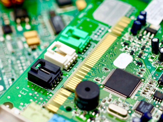
The purpose of a printed circuit board is to hold an electronic circuit together. When all the different components are attached to it, it is called a printed computer circuit board assembly, or PCBA. A PCB with multiple layers can contain as many as ten stacked PCBs. This allows for the formation of a three-dimensional electronic circuit.

Components of A Circuit Board

Components soldered onto the PCB are essential for conducting electricity on the boards.

Some of the components included on a computer circuit board includes:

  • Transistors are the most important part of an electronic circuit and can be described as tiny switches that are triggered by electric signals. They are the basic building blocks of microchips. Working alongside these are more passive elements like resistors and capacitors.
  • Resistors apply a specific amount of resistance to the current. They transmit the electric current to produce voltage.
  • Capacitor stores electric charge in the board and releases it when power is needed.
  • Inductors store energy as a magnetic field and block interference signals in the board. Small circuits, commonly labeled “micro-electric,” don’t use inductors very often.
  • Diodes control the flow of electricity making it only flow in one direction to avoid causing damage.

The most advanced designers of computer circuit boards use computer-aided design programs or CAD. These are the most realistic way to design circuit boards because of the complexity of digital computers- as they use millions of transistors.

One of the best ways to understand the products we create for your every need is to study the basic components. The world of circuits and circuit boards is vast and there is always something new to learn. Whether it’s an advancement or yet another element of your printed computer circuit board project.

Types of PCBs

There are several different types of PCBs you can choose from depending on your planned usage.

These consist of:

  • Single-sided PCBs – Most commonly used type of PCB used with almost any electronic circuitry
  • Double-sided PCBs – The components are on both sides of the PCB, used for more complex circuitry, and is slightly more expensive
  • Multi-Layer PCBs – Combines two double-sided circuits, used in most electronic devices
  • Rigid PCBs – Made out of thermoplastic material, the most durable, and often used in military technology
  • Flex Circuits – Uses flexible material in smaller assemblies for simple electronics
  • Rigid-Flex PCBs – A combination of both the rigid and flex PCBs, providing both flexibility and durability
  • High-Frequency PCBs – Used for circuits that have fast microprocessors for high productivity computers
  • Aluminum PCBs – Uses an aluminum backing to add more strength when there is a lot of electromagnetic energy

A computer circuit board specialist can help you determine which type is right for you depending on the application of your PCB.

Design and Manufacture Your PCB With Hallmark Nameplate

You can learn more about our PCB (Printed Circuit Board) Assembly Services by visiting our website. Our team will help walk you through the electronic assembly process and answer all your questions.

Find the perfect solutions for your needs, request a FREE quote today!